HC11 SPI Design Example
This document describes the VHDL behavioral design of the Serial Peripheral
Interface (SPI) Unit of the Motorola HC11 microcontroller. The SPI provides
synchronized communication between the HC11 microcontroller and peripheral
devices or other microcontrollers. The example will proceed by first
describing the operation of the SPI, and then looking at the behavioral
design of the SPI.
Operation of the HC11 SPI
This description is based on the M68HC11 Reference Manual. The SPI subsystem
performs synchronous master/slave type exchange of two data bytes (8 bits).
Both master and slave units contain an 8 bit shift register. During a
transfer,
incoming bits are shifted into the masters 8 bit register, while the old
values,
are shifted out to the slave. When connected together the master and slave
shift registers form a circular 16 bit shift register. During transfer,
the contents of the 16 bit shift register is shifted by 8 bits, exchanging
the two values in master's and slave's registers. The shift register is
controlled by a single clock provided by the master.
Two controls select the format of the transfer, the clock phase control bit
(CPHA), and the clock polarity control bit (CPOL). The CPOL selects an
active high or an active low clock. The CPHA controls how the start
of the transfer is defined for the slave unit. If CPHA is '0', then
the slave begins transfer as soon as the SS line (controlled externally) is
active low. If CPHA is '1', then the transfer begins on the first edge of the
master's serial clock (SCK). These two formats have a large impact on how the
shift registers are clocked from the master's serial clock. The impact
of the two formats is discussed more later.
The serial clock used for transfer is derived from an internal clock (PH2) of
the HC11. This clock is divided by 2,4,16, or 32 depending on the value
of the two SPI Bit Rate control bits (SPR1 and SPR2).
The master or slave mode of the SPI is determined by the master/slave mode
control bit (MSTR). The SPI can be enabled or disabled by the SPI system
enable control bit (SPE). The SPI will also generate an interrupt to
the HC11 CPU when a data transfer has been completed, if the SPI interrupt
enable control bit (SPIE) is set. Regardless of the value of the SPIE
control bit, the SPI transfer complete flag (SPIF) is set when a transfer
in complete.
Design of the HC11 SPI
The VHDL design of the SPI consists of three parts.
- hc11type.vhd contains common VHDL type
definitions used by all the components of the HC11.
- hc11clk.vhd contains the behavioral
design of the HC11's internal clocks.
- hc11spi.vhd contains the behavioral design
of the SPI subsystem itself.
Before examining the design of the SPI subsystem, we will first turn our
attention to the two support files, hc11type.vhd and hc11clk.vhd.
The hc11type module contains a VHDL package which defines several common
types that are used by the entire HC11 design. The byte and word
types represent 8 bit and 16 bit vectors. The byte_array and word_array
types are defined for use with the resolution functions that follow.
Several resolved signal types are defined with the resolution functions.
The databus type is the only one used by this example. The databus
type is used to represent the HC11's system data bus that can be driven
by many parts of the design.
The hc11clk module contains a component that generates the internal clocks
use by the HC11. All of the internal clock signals are derived from a single
external crystal. Since the frequency of this main clock depends on
external circuitry, the frequency value is configured with a generic.
The generic Tcycle is the length in nanoseconds of this clock's cycle.
The use of the generic Tcycle allows the same entity (clock) to be
used in several designs with different frequencies. This is a good practice
because only one entity has to be designed, which saves time, and it is also
easier to maintain one design than several.
The architecture of the clock design contains
simple signal assignments to create clocks with different phases and multiples
of the crystal frequency. The gen_extal process is a typical
implementation of a clock
signal. It contains a single signal assignment that creates one cycle of the
clock. The cycles of the clock are then repeated with the use of the wait
statement. The wait statement will suspend the process for Tcycle
time units.
Thus, the process will resume every Tcycle time units and the
signal assignment will create that cycle each time.
The gen_clock process is used to generate several clocks, since they
all have the same period. There is a lot of simulator overhead in suspending
and resuming processes, so combining these signal assignments into a single
process is much more efficient than using separate processes. This is
especially important with the clock signals because they change the most
frequently, which means they require the most processing by the simulator.
Now we return to the discussion of the design of the SPI subsystem itself.
The first step of the design process is to draw a block diagram of the
system begin designed. This is the block diagram of the SPI used for
our VHDL design.
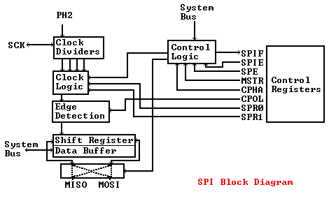
The Clock Dividers block generates 4 clocks that are derived by dividing the
HC11's internal PH2 clock by 2,4,16, and 32. The Clock Logic block then
selects one of these clocks (in master mode) or the SCK input pin (in slave
mode) depending
on the value of SPR0,SPR1, and MSTR. This block is enabled by the Control
Logic block. When the output from the Clock
Logic block is enabled, it will clock the shift register performing the
data transfer. The shift in/out pins of the SPI subsystem depend on the
master/slave mode of the system. The MISO pin is used for input when
configured in the master mode and output when configured in the slave mode.
Similarly, the MOSI pin is used for output when
configured in master mode, and input when configured in slave mode.
The Control Logic block of the SPI controls the overall operation of the
subsystem.
The first part of the VHDL model is the entity declaration for the SPI
subsystem. The first part of the entity declaration is the port clause
describing the interface to the spi entity. The first three signals
(E,ph1, and ph2) are internal clocks signals.
The reset signal is a global asynchronous reset for the entire HC11.
The ss signal is an external input pin of the HC11 used to control the
slave's operation. Depending on the mode (master/slave) of the SPI, it
may output or input the SCK signal. The SCK signal is an external
bidirectional pin of the HC11. Since all the pin I/O logic of the HC11
is separated into their own entities, the SPI has two separate signals for
input and output. The direction and signal driving the external pin is
then controlled by the external pin logic (which is not part of this example).
For the same reason that the SCK signal is separated into input and output
signals, the MISO and MOSI pins are separated into input and output signals.
These signals are defined as mi,si,mo, and
so.
The next two signals are used for mode fault detection. A mode fault
occurs when the HC11 is configured in master mode and the SS pin is driven
active low (selecting slave operation). If the external SS pin is configured
for input, then mode faults will be detected. The active high ss_dir
signal, driven by the external I/O pin logic, indicates when the SS pin is
configured for input. The mfault output signal will then be set
active high, if a mode fault occurs. The int_spi signal is the
internal interrupt request line to the CPU. The status of the SPI subsystem
(enabled/disabled and master/slave mode) is used by other subsystems of the
HC11, so these control bits are output with signals spe and
slave. The remaining signals in the port clause define the signals of
the HC11's system bus.
Following the port clause are two sections of constant definitions.
These constants are defined in the entity declaration because they are
independent of the implementation of the architecture. This means that if
there
is more than one architecture for the spi entity, these constants would be
the same. Since they are the same for every architecture body, they can
be put in the entity declaration. This saves the trouble of redeclaring them
in every architecture body. The first set of constants define the bit
positions of the SPI control bits within the HC11's registers. All of the
control bits and flags in the HC11, that are accessible to the CPU, are made
accessible via a memory mapped block of registers. The reg_en
input signal is active during a bus cycle that accesses one of the memory
mapped registers. This is discussed more later. The second set of
constants define the states of a finite state machine (FSM) used to control
the SPI subsystem.
Immediately following the entity declaration is an architecture
body of the spi entity. This architecture declares several internal signals,
which will be discussed as needed. The first four statements of the
architecture connect internal signals to some of the output signals of the
entity. The SPCR bit vector referenced in the last two of these signal
assignments represents one of the memory mapped registers of the HC11. This
is the SPI Control Register. The next signal assignment selects mi
or si as the input for the shift register depending on the mode
(master/slave) of the SPI. The process following that selects mo or
so for output in a similar way. A process is used because it
is more convenient to write. The next signal assignment drives the interrupt
request line whenever it is enabled by the SPIE control bit and a transfer
has been completed (indicated when SPIF is active high) or when a mode fault
has occured (indicated when MODF is active high).
The next section implements the clock related blocks in the block diagram of
the SPI subsystem. The first is the Clock Dividers block. This block is
implemented using a binary counter. Each bit of the clock value is the next
less significant bit divided by 2. The least significant bit is the signal
clocking the counter (PH2) divided by 2. The 5 bit counter output represents
a divide by 2 chain, dividing the PH2 clock by the multiples 2,4,8,16, and
32. Since only the signal divided by 2,4,16, and 32 are needed they
are assigned, in order, to the prescaled bit vector. The
SPR0 and SPR1 bits are then be used to index the prescaled bit vector.
Thus, spi_clk is the clock rate selected by SPR0 and SPR1.
The main_clock process, which follows in the source code, selects
the proper clock
to use for transfers and determines whether the clock is enabled or not. If
the SPI is in the transmitting state, it must be configured as a master
and the master uses the internally selected spi_clk for driving
the shift register. If the SPI is in the receiving state, it must
be configured as a slave and uses the clock generated by the master, which
is input via the sckin signal.
The next section of the implementation is somewhat more complicated than
one would expect due to the different configurations possible for
clock polarity (CPOL) and clock phase (CPHA). This section implements the
Edge Detection block directly driving the shift register. The
first statement creates the shift_edge signal for convenience. This
signal determines which edge (rising/falling) causes the register to shift,
which depends on the configuration of CPOL and CPHA. The next statement is
the count process, which counts the number of edges and is reset
between transfers. The value of this counter will be used later to control
the shift register. It is really part of the Control Logic block of our
diagram though.
The next process is the main component of the Edge Detection block.
It is complicated due to the fact that when the clock
phase is '1' the register is shifted on the second edge of the clock, instead
of the first, and there is no edge for the last bit that must be shifted. The
shift signal is the output from this process and is used to drive
the shift register. The first step is to detect the correct rising or
falling edge. This is done with the first if statement. If the right
edge has occurred, then we shift under two conditions. First, when the
clock phase is '0' and second, when
the clock phase is '1' and this is not the first edge (no_bits/=0), since
in this mode the first edge does not cause a shift. These two cases are
handled by the second if statement. The elsif part of the first if
statement handles shifting the last bit during a transfer where the clock
phase is '1', since there is no clock edge for this last bit. It causes
a shift to take place when the FSM has recognized the end of a transfer
(i.e. when the SPIF flag is set) and the clock phase is '1'.
The next process, do_shift, implements the shift register of the SPI
subsystem. The shift register is loaded with a value via the memory mapped
register SPDR (SPI Data Register) at register block address 2A. Thus,
the first part of this process transfers data from the system bus to the
shift register during a write cycle to register block address 2A.
The wr_enable signal is described later. The shift
signal is then used to actually shift the contents of the register
as controlled by the process discussed in the last paragraph. The
for loop used here to do the shift employs a good common practice of
denoting the bounds of the vector with byte'high and byte'low instead
of 7 and 0 because these may change. Rather than change the references
to 7 and 0 everywhere in the source code, the high and low attributes are
used and will never need to be changed.
This process additionally sets the internal signal SPDR_full, when new data
is loaded into the SPDR register. This is signal is used in the FSM to start
a transmission, when configured in master mode.
The next process is concerned with the FSM that controls the state of the
SPI subsystem. The process detects the beginning of a transfer in slave mode.
In master mode, a transfer begins when the SPDR register is written by the
CPU. For the slave, the beginning of a transfer is detected differently
depending on the clock phase. If CPHA is '0', the transfer begins
on the falling edge of the external input pin SS. Otherwise, the
beginning of a transfer is detected by the first edge on the external
SCK input pin. This process and the remaining processes are part of the
Control Logic block of the block diagram.
The state of the SPI is controlled by a finite state machine defined in the
fsm process. There are many different ways to implement finite
state machines in VHDL. This FSM is implemented entirely in one process.
On each falling edge of ph2 the next state is determined, and
certain actions are taken, when the state changes. The following is
a diagram of this FSM.
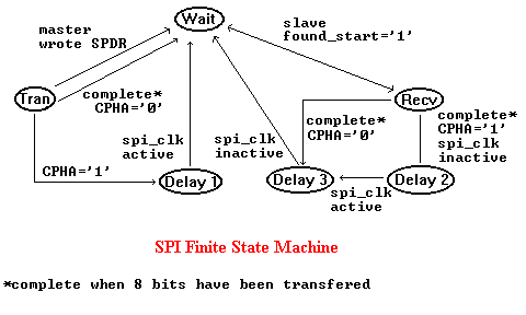
There are two main actions that take place in this process due to state
changes. The first is a read buffer for the SPDR (shown in the block
diagram with the shift register). When a transfer is complete, the value of
the shift register
is latched into the read buffer. When the CPU writes to the SPDR, it writes
to the shift register, but when it reads the SPDR, it reads from this
read buffer. This means that another transfer can begin before the CPU
reads the result of the last transfer. The second is to set the SPIF flag.
Since signals may only have one driver, unless they are resolved, all changes
to SPSR are made in one process controling the SPSR. In order to set the
SPIF flag, an intermediate signal is used, set_SPIF. A rising edge of this
internal signal will cause the SPIF bit to be set within the process
controlling the SPSR (discussed later).
The delay states, in the FSM, are used to synchronize the
completion of the transfer.
The SPCR register is controlled by the SPRC_register process.
If a mode fault has occured (rising edge of MODF), the SPI is automatically set
to slave mode to avoid conflicts on the external pins. The first if statement
checks for mode faults and clears the MSTR bit, when one has occured.
Otherwise the process merely writes the bus data to the register when the CPU
writes to its memory mapped address. The SPSR_register
process controls the SPSR register in a similar manner, except the bits of
the SPSR may also be controlled via the internal signals set_SPIF and
set_MODF, as mentioned in the last paragraph.
The next process detects the mode faults mentioned at the beginning of
this discussion. When a mode fault is detected, the MODF bit of the SPSR
is set indirectly with the set_MODF signal.
The last process is bus_cycle. This process
handles some general control of the bus cycle and all reads of the
SPI related memory mapped registers. Writes to the SPI register are handled
in separate parts of the implementation due to the problem of only having
one driver, which was mentioned earlier. However, this is not a problem with
reading signals, so the CPU reads of the registers are all handled in one
process. The first statement, the wait statement, waits for the falling
edge of the address strobe signal as. At this time the
address and r/w lines of the system bus are valid. The address is latched into
the address latch. The rd_enabled and wr_enabled
are also latched based on the value of the r/w line and reg_en
signal.
The next wait statement waits for the rising edge of the ph1 signal.
At this point read data should be placed on the bus. If this is a read and
the address is any of the SPI register, their values are used to drive the bus.
If one of these registers is read, another wait statement is used to wait for
the falling edge of ph1. At this point the bus data drivers are
removed because the data valid period is complete.
A Test Bench for the HC11 SPI VHDL model
The spitest.vhd file contains a VHDL test bench
that verifies some of the operation of the SPI subsystem. It is always best
to create a test bench for each VHDL entity you create before continuing to
design. Otherwise, it is difficult to isolate a problem in a large design
containing several untested entities.
To compile and test the
VHDL model of the SPI, execute the following commands from DOS in the
examples subdirectory of directory where you installed the compiler.
vhdl hc11type
vhdl hc11clk
vhdl hc11spi
vhdl spitest
link spi spitest test_spi
sve spi spi.env
Copyright 1995, Green Mountain Computing Systems.
Copying this document is strictly prohibited. Making any non-volatile or
semi-permanent copies of this document is a violation of international
copyright laws.